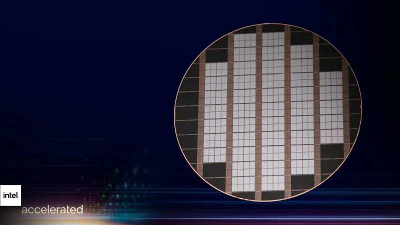
“There is growing demand for computing power driven by the digitization of everything, but until now fabless customers have had limited options for designing around the most advanced mobile technology,” Pat Gelsinger, CEO of Intel Corporation said. “Intel’s collaboration with Arm will expand the market opportunity for IFS and open up new options and approaches for any fabless company that wants to access best-in-class CPU IP and the power of an open system foundry with leading-edge process technology.” Intel and more specifically, Intel Foundry Services (IFS), elaborates further that its partnership with ARM is part of its IDM 2.0 strategy, which includes investing in leading-edge manufacturing capacity around the world, including significant expansions in the US and the EU. For context, the 18A process refers to the chipmaker’s ability to make chip wafers at the thinner-than-DNA 1.8nm process. One of the benefits of Intel’s 18A process is that it can be optimised to extract PPAC advantages out of the node, thanks on no small part of it using Gate-All-Around (GAA) transistors, otherwise known by Intel’s own name for the process, RibbonFET. Another benefit of GAA transistors is PowerVia, which is a Power Delivery Network (PDN) that can allow mobile SoCs to be optimised for burst behaviour, while datacentre SoCs can be optimised for constant high loads.
“Arm’s secure, energy-efficient processors are at the heart of hundreds of billions of devices and the planet’s digital experiences,” Rene Haas, CEO of ARM says. “As the demands for compute and efficiency become increasingly complex, our industry must innovate on many new levels. Arm’s collaboration with Intel enables IFS as a critical foundry partner for our customers as we deliver the next generation of world-changing products built on Arm.” (Source: Intel PR, Tom’s Hardware)

