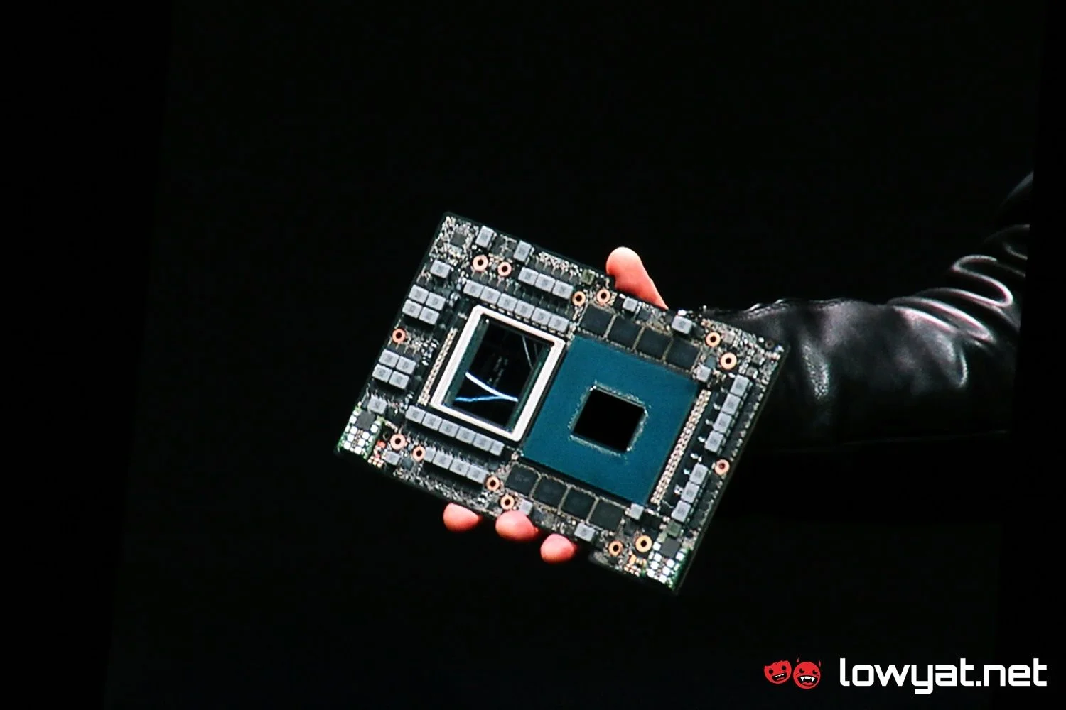
As per the official product page of the GH200, the new superchip was designed from the ground up, for the purpose of both giant-scale Generative AI and high performance computing (HPC) applications.
“Generative AI is rapidly transforming businesses, unlocking new opportunities and accelerating discovery in healthcare, finance, business services and many more industries,” Ian Buck, vice president of accelerated computing at NVIDIA, says. “With Grace Hopper Superchips in full production, manufacturers worldwide will soon provide the accelerated infrastructure enterprises need to build and deploy generative AI applications that leverage their unique proprietary data.” Specs-wise, the GH200 superchip can boast a 72-core count, all of which are ARM’s Neoverse V2 cores, a 117MB L3 Cache, up to 480GB LPDDR5X, up to 512GB/s memory bandwidth, and up 4x PCIe Gen5 links. And those details are just for the Grace CPU. The second half of the superchip is the Hopper H100 GPU, and that itself is a beast.
The H100 GPU of the GH200 comes with up to 96GB of HBM3 memory, which translates to a 4TB/s memory bandwidth at peak performance. There is also the NVLink-C2C CPU-to-GPU bandwidth which can reach 900GB/s and is bidirectional. As for the power consumption, NVIDIA basically allows consumers to program the chip to run between a 450W and 100W power envelope. Additional performance details of the GH200 include 67 teraFLOPS for FP64 Tensor cores but up to 989 teraFLOPS with the TF32 Tensore Cores. Oh, and NVIDIA says that you can choose between air-cooling or liquid-cooling.
As for availability, the NVIDIA GH200 Grace Hopper Superchips are expected to hit the market later this year, although no specific date has been given. (Source: NVIDIA)


